
Comparison of PLL Architectures
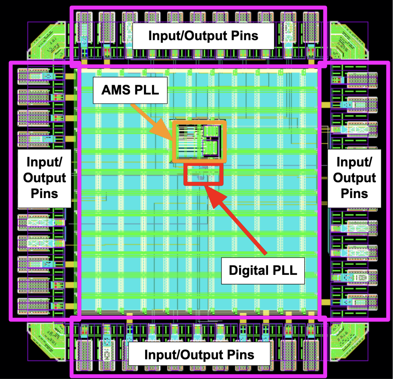
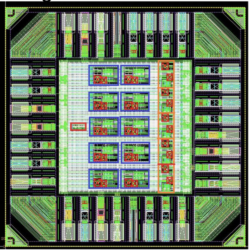
Designed and fabricated a 1 mm² TSMC 28 nm chip integrating both an all‑digital and an analog/mixed‑signal phase locked loop
Verilog Virtuoso Genus Innovus TCL
HWE Intern - SoC Design
May 2025 – Aug 2025

HWE Intern - SoC Design
May 2025 – Aug 2025HWE Intern - Yield Engineering
Jun 2024 – Aug 2024
HWE Intern - Yield Engineering
Jun 2024 – Aug 2024SWE Intern - Systems R&D
May 2023 – Aug 2023

SWE Intern - Systems R&D
May 2023 – Aug 2023SWE Intern - Automation
May 2022 – Aug 2022
SWE Intern - Automation
May 2022 – Aug 2022 Designed and fabricated a 1 mm² TSMC 28 nm chip integrating both an all‑digital and an analog/mixed‑signal phase locked loop

Analyzed half‑million‑row wafer datasets to predict defective chips using feature engineering, CatBoost modeling, and cost‑optimized thresholding, improving defect detection and reducing manufacturing losses.
Pixel image sensor interface in TSMC N65
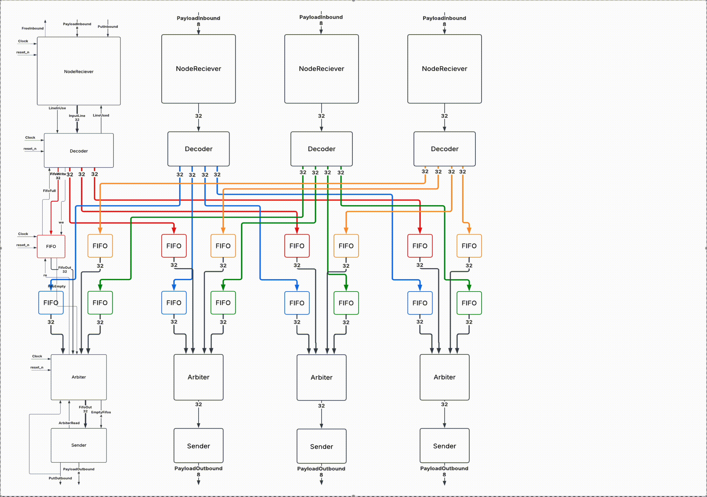
Built high‑performance hardware systems, including a fast matrix calculator, a network‑on‑chip, and a USB 2.0 protocol engine